| 108-Layer PCB, Rigid-Flex & 5G PCB Manufacturing | Pengsheng's High-End Solu |
| Date:2025-06-04 20:46:37 | Visits: |
Why do high-end manufacturing and large-scale production become the core competitiveness of the PCB industry?
Today, with the explosive development of technologies such as 5G, AI, and the Internet of Things, electronic devices are evolving towards miniaturization, intelligence, and high reliability. This poses dual challenges to the performance and production capacity of PCBs.
The demand for high-end manufacturing has surged: communication base stations require high-frequency and high-speed boards that support millimeter-wave signal transmission, medical equipment relies on multi-layer boards that can withstand extreme environments, and automotive electronics demand high-reliability circuit boards that comply with the IATF 16949 standard. According to the 2024 report by Prismark(https://www.prismark.com), the global high-end PCB market is growing at an annual rate of 15%, with 5G communications and automotive electronics accounting for over 40% of the demand.
Mass production becomes a must: The annual shipment of tens of millions of devices by consumer electronics brands requires PCB suppliers to have a stable monthly production capacity of tens of thousands of square meters. Data from the China Printed Circuit Association (CPCA) shows that the proportion of large-scale orders in the global PCB market rose to 68% in 2023, making large-scale production capacity a key factor for enterprises to capture the market.
As a leading enterprise deeply rooted in the PCB industry, Pengsheng Technology drives its development with a dual strategy of "technology + capacity", accurately grasping the pulse of the industry and providing global customers with full-chain solutions ranging from high-end customization to large-scale mass production.
II. High-End Manufacturing: Five Core Technologies Redefining Industrial Boundaries
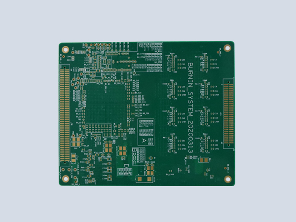
1. High-layer PCB: Pushing the Limits of Layer Count
Pengsheng Technology's high multi-layer boards can reach up to 108 layers, using laser drilling and automatic alignment technology. The minimum line width / line spacing is 3 mil, meeting the complex circuit requirements of supercomputers and data centers. A typical case is a 48-layer backplane customized for a European server manufacturer. Through a 25:1 high aspect ratio design, signal delay was reduced by 20%, making it a core component of cloud computing infrastructure.
2. High-frequency/High-speed PCB: Unleashing New Dimensions in Communication
• Material breakthrough: Low-loss dielectric materials such as Rogers and PTFE are selected, supporting 28GHz millimeter-wave signal transmission for 5G base stations, with signal loss < 1.2dB/in (10GHz).
• Process Innovation: Pengesheng has achieved a line width accuracy of ±8μm by employing LDI laser exposure and blind via technology, which has been successfully applied to the antenna module of satellite communication PCBs, helping our customers gain an early advantage in 6G research and development.
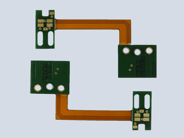
3.Rigid-Flexible PCB: The Future of Flexible Electronics
SourceURL:file:///Users/liaozh/Library/Containers/com.tencent.xinWeChat/Data/Library/Application Support/com.tencent.xinWeChat/2.0b4.0.9/786c5c584a82659ce54e293c8c082b2b/Message/MessageTemp/9e20f478899dc29eb19741386f9343c8/File/High-End PCB Manufacturing & Mass Production Pengsheng Technology's 5G & Automotive Solutions.docx Pengsheng's rigid-flex boards can be integrated up to 16 layers (8 layers of flexible material), with a minimum line width of 2.5 mils. They can withstand over 100,000 bends and are widely used in wearable devices and automotive electronics. In a German autonomous driving project for ADAS sensor rigid-flex PCBs, its rigid-flex boards passed environmental tests ranging from -40°C to 125°C, ensuring the stable operation of sensor wiring harnesses in complex road conditions.
4. HDI boards (HDI PCB): Innovation in High-Density Integration
Supports 3 + N + 3 stacking structure, with a minimum aperture of 0.08mm and a line width / line spacing of 3mil/3mil. Mainly serves AI chip packaging and high-end mobile phone motherboards. In 2023, Pengsheng's HDI Level-4 process went into mass production, helping an Asian mobile phone brand reduce the motherboard area by 35% and increase battery life by 18%.
5. Industry-customized solutions: Precisely matching vertical demands
Medical PCB: Certified by ISO 13485, it adopts lead-free technology and biocompatible coating, meeting the strict safety requirements for implantable devices.
• Industrial PCB: With vibration-resistant and electromagnetic interference-proof design, it is suitable for industrial robot controllers in smart factories, featuring an average mean time between failures (MTBF) of over 100,000 hours.
III. Mass Production: The Efficiency Revolution Behind Scale-up
Capacity layout and automation upgrade Pengsheng's two factories in Shenzhen cover a total area of 20,000 square meters and are equipped with over 60 advanced machines, including fully automatic electroplating lines, LDI exposure machines, and high-speed drilling machines, achieving:
• Sample prototyping: Handle 6,000 types of samples per month, with the fastest delivery within 24 hours.
Batch production: Monthly production capacity reaches 60,000 square meters, meeting the delivery requirements of communication equipment manufacturers for single orders of 100,000 pieces.
2. Large-scale cases in the communication field: Global competitiveness of 5G PCBs
As a core supplier for mainstream communication equipment manufacturers, Pengsheng has customized a 5G NR base station PCB with a 22-layer design for them, supporting Massive MIMO antenna arrays and integrating over 3,000 RF units on a single board. By optimizing the production process, the mass production yield of this product has been increased to 98.5%, the cost has been reduced by 15%, and the annual shipment volume exceeds 500,000 pieces.
3. Mass Delivery of Automotive Electronics: Quality Assurance under the IATF 16949 System
Pengsheng Auto's PCB production line strictly adheres to the IATF 16949 standard, implementing 100% traceability from raw material procurement to finished product testing. In 2023, the monthly shipment volume of ADAS sensor PCBs supplied to a certain new energy vehicle manufacturer exceeded 800,000 pieces, with a defect rate of less than 0.5%, successfully entering the European supply chain system.
IV. PENGSHENG TECHNOLOGY: A One-Stop Partner Capable of Both High-End and Bulk Production
From the technological breakthrough of 108-layer high multi-layer boards to the production capacity of 60,000 square meters per month, Pengsheng Technology has built its core barriers with "military-grade quality + flexible manufacturing".
Certification endorsement: Our products have passed multiple certifications including UL, CUL, IATF 16949, GJB 9001C, etc., and comply with standards in over 30 countries in Europe, America, Asia and other regions.
Global Services: Our overseas business department directly serves customers in Europe and America. We respond to inquiries within 2 hours, provide customized solutions within 48 hours, and have shortened the average delivery cycle to 12 days.
If you are looking for PCB manufacturers or suppliers that combine technical depth with large-scale production capacity, welcome to visit Pengsheng Technology's official website at www.ppcircuits.com to explore more possibilities of high-end manufacturing and large-scale production. |
| Prev:PSTECT Launches Marine-Grade PCBA Solution to Boost Coastal Smart Industry Upgra Next: |